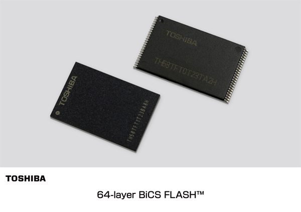
Toshiba Corporation today unveiled the latest generation of its BiCS FLASH three-dimensional (3D) flash memory with a stacked cell structure*1, a 64-layer device that will be first*2 in the world to start sample shipments today. The new device incorporates 3-bit-per-cell (triple-level cell, TLC) technology and achieves a 256-gigabit (32gigabytes) capacity, an advance that underscores the potential of Toshiba’s proprietary architecture. Toshiba continues to refine BiCS FLASHTM, and the next milestone on the development roadmap is a 512-gigabit (64-gigabytes) device, also with 64 layers.
The new device succeeds the 48-layer BiCS FLASHTM, and its leading-edge 64-layer stacking process realizes a 40% larger capacity per unit chip size than 48-layer stacking process, reduces the cost per bit, and increases the manufacturability of memory capacity per one silicon wafer. 64-layer BiCS FLASHTM can meet demanding performance specs, and the new device will be used in applications that include enterprise and consumer SSD, smartphones, tablets and memory cards.
Since announcing the world’s first*3 prototype 3D flash memory technology in June 2007, Toshiba has continued to advance development. The company is actively promoting BiCS FLASHTM to meet demand for larger capacity with smaller size.
Toshiba will produce the new 64-layer BiCS FLASHTM in the New Fab 2 at Yokkaichi Operations, which was officially opened earlier this month, and mass production of 64-layer BiCS FLASHTM is scheduled to start in the first half of 2017. |